PCB Design in 2026: HDI, Embedded Components, and the Death of Simple Boards
The humble printed circuit board, the green rectangle that has been the foundation of electronics for over sixty years, is undergoing its most radical transformation since the introduction of surface mount technology in the 1980s. Driven by the relentless demands of miniaturization, performance, and cost reduction, PCB technology in 2026 is entering territory that would have been considered science fiction a decade ago.
The HDI Revolution
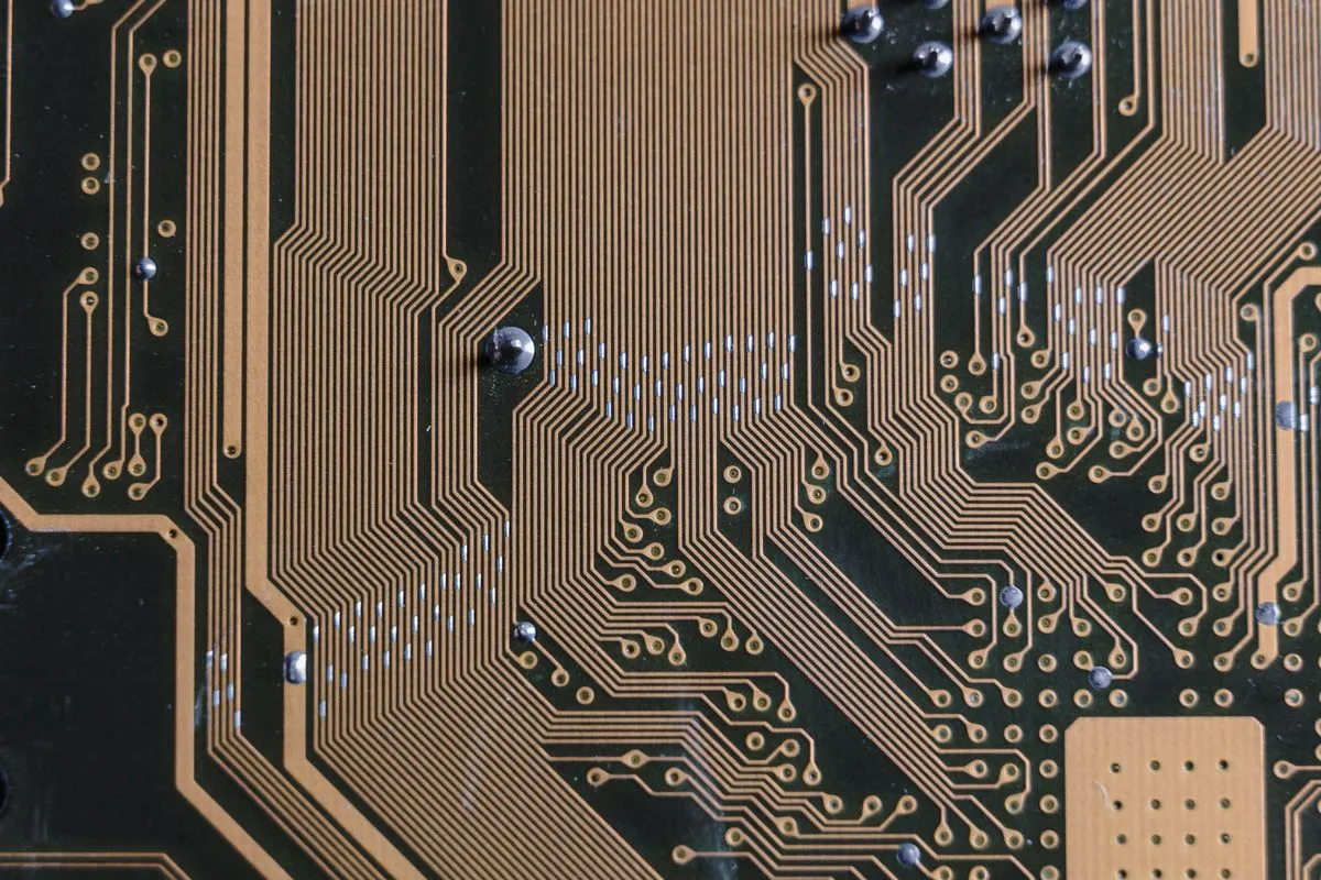
High-Density Interconnect (HDI) technology, characterized by microvias (< 150μm diameter), fine lines/spaces (< 75μm), and thin dielectrics, has moved from a niche technology used in smartphones and military systems to a mainstream requirement for an expanding range of applications.
The driver is simple: component density. Modern BGA packages with 0.4mm ball pitch require routing densities that are physically impossible with traditional PCB technology. A 400-ball FPGA on 0.5mm pitch generates a routing challenge that demands at least 4-6 layers of HDI construction: microvias, stacked vias, and sequential lamination.
But HDI is not just about routing density. It also enables dramatic improvements in signal integrity for high-speed designs. Shorter via stubs, reduced parasitic capacitance, and tighter impedance control translate directly into better performance at multi-gigabit data rates. For designs targeting PCIe Gen 5, DDR5, or 100G Ethernet, HDI is not optional; it's a prerequisite.
The Design Challenge
HDI design demands a fundamentally different approach to PCB layout. Traditional PCB design is essentially two-dimensional: the engineer places components on the top surface and routes connections through layers below. HDI design is three-dimensional. The engineer must think about via stacking strategies, sequential lamination build-ups, and the interaction between mechanical stress and microvia reliability.
The design rules are also dramatically tighter. Where a traditional PCB might specify 150μm traces with 150μm spaces, an HDI design might require 50μm traces with 50μm spaces, tolerances that approach the capability limits of most PCB fabricators. Designing to these limits without intimate knowledge of your fabricator's capabilities is a recipe for yield problems and delays.
Embedded Components: The Third Dimension
The next frontier in PCB evolution is embedded component technology: literally burying passive components (resistors, capacitors, inductors) and even active components inside the PCB substrate. This technology, which has been in development for over a decade, is finally reaching commercial maturity.
The benefits are compelling. Embedding decoupling capacitors inside the PCB, directly beneath the BGA pads of a processor, reduces the parasitic inductance of the power delivery network by 50-70% compared to surface-mounted capacitors. For high-performance digital designs, this translates into cleaner power delivery, reduced electromagnetic emissions, and the ability to operate at higher clock frequencies.
Embedded resistors, typically implemented as thin-film resistive layers in the PCB stackup, eliminate hundreds of surface-mounted resistors from high-density designs. This recovers precious PCB area for routing and improves reliability by eliminating solder joints.
The Traceability Challenge
Embedded components create a unique traceability challenge. In a traditional design, every component is visible and inspectable. An embedded capacitor, buried inside the PCB substrate, cannot be visually inspected, probed, or replaced. Its quality must be guaranteed by process control during fabrication, not by inspection after assembly.
This means that the engineering data package for a PCB with embedded components must include not just the traditional Gerber files and pick-and-place data, but also detailed specifications for the embedded component materials, processes, and quality controls. The traceability chain extends from the design intent through the material selection to the fabrication process parameters, a chain that traditional PCB design tools are poorly equipped to manage.
RF Integration: When Every Trace Is an Antenna
The proliferation of wireless connectivity (Wi-Fi 7, 5G, UWB, Bluetooth LE, Matter) means that an increasing percentage of hardware products must integrate RF functionality onto their main PCB. What was once the domain of specialized RF engineers working on dedicated radio modules is now a mainstream PCB design challenge.
RF design on a mixed-signal PCB is notoriously difficult. Every trace is a potential antenna. Every via is a potential resonant cavity. Every ground plane discontinuity is a potential radiation source. The electromagnetic environment inside a dense, multi-layer PCB is ferociously complex, and simulation tools, while improving, still struggle to capture all of the relevant interactions.
The practical implication is that PCB designs with integrated RF sections require significantly more design-for-manufacturing collaboration between the PCB designer, the RF engineer, and the fabricator. Stackup selection, material choice (standard FR-4 vs. low-loss PTFE composites), and layer assignment all affect RF performance in ways that are difficult to predict without simulation and empirical validation.
The Skills Gap
The rapid evolution of PCB technology is creating a significant skills gap in the industry. Many experienced PCB designers were trained on through-hole and basic surface-mount technology. The jump to HDI, embedded components, and integrated RF requires new knowledge in materials science, electromagnetic theory, and manufacturing processes that these engineers may not possess.
At the same time, the design tools are evolving rapidly. Modern PCB design tools include integrated 3D electromagnetic simulation, automated HDI via assignment, and embedded component libraries. But these features are useless if the designer doesn't understand the underlying physics well enough to interpret the results.
The Documentation Burden
As PCB complexity increases, so does the documentation burden. A simple 4-layer PCB might require a fabrication drawing, a stackup specification, and a bill of materials. A complex HDI board with embedded components requires all of that plus detailed microvia specifications, sequential lamination instructions, embedded component material specifications, impedance control requirements, and cross-section analysis criteria.
Managing this documentation (and maintaining traceability between the design intent, the fabrication specification, and the quality requirements) is becoming a significant engineering challenge in its own right. The PCB design file is no longer sufficient as the master engineering document. It must be connected to a broader engineering data model that captures the full context of the design.
Looking Ahead
The PCB of 2030 will look nothing like the PCB of 2020. Embedded active components, optical interconnects, and flexible-rigid constructions with integrated sensors will transform the circuit board from a passive interconnect substrate into an active functional element of the electronic system.
For hardware engineers, this means that PCB design is no longer a commodity skill that can be outsourced to the lowest bidder. It is a core engineering discipline that demands continuous learning, deep collaboration with fabricators, and engineering infrastructure that can manage the escalating complexity. The engineers and teams that embrace this evolution will build the next generation of electronic products. Those that don't will find themselves increasingly unable to compete.